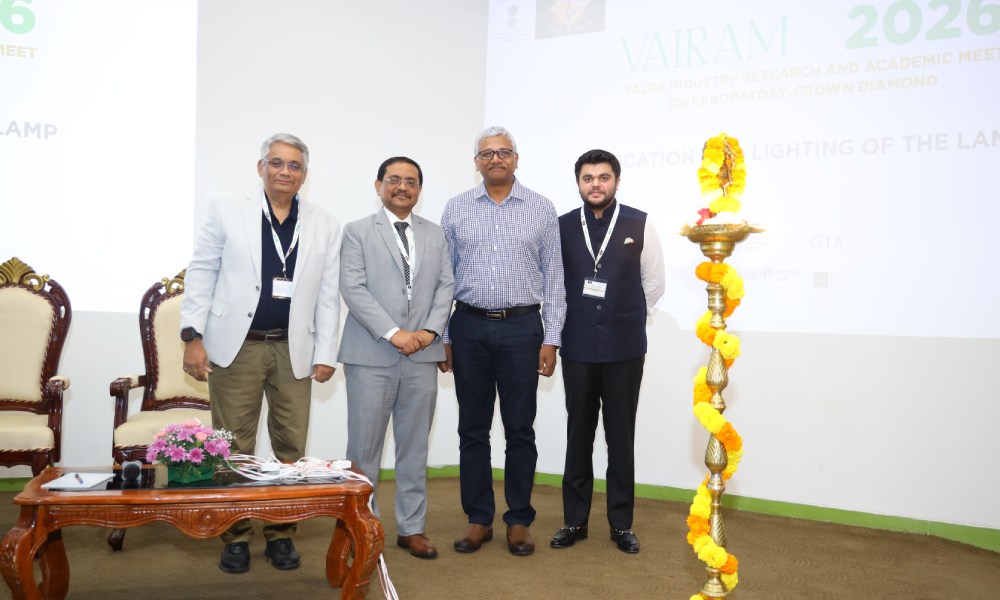
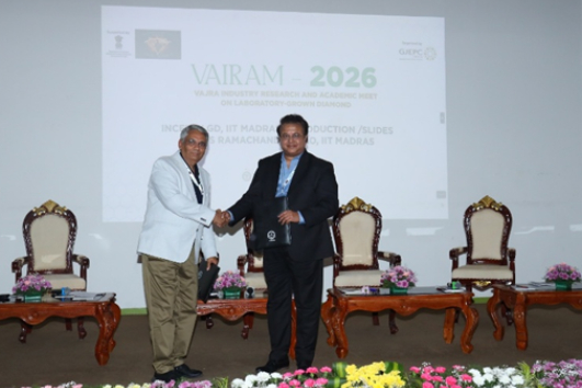
The Vajra Industry Research & Academic Meet (VAIRAM) Workshop 2026, co-organised by GJEPC and InCent LGD IIT Madras, was held on 20 February 2026 at IIT-Madras, Chennai, with stakeholders from academia and industry discussing the next phase of India’s laboratory-grown diamond (LGD) growth.
The dignitaries present at the opening ceremony were Prof. Manu Santhanam, Dean (IC&SR), IIT Madras; Sanket Patel, Convener – LGD Committee, GJEPC; M.S. Ramachandra Rao, Head of the India Centre for Lab Grown Diamond (InCent-LGD) at IIT Madras; Jayanti Savaliya – Gujarat Region Chairperson, GJEPC; Ashish Borda, Convener – PMBD, GJEPC; Mital Doshi, Convener, BITC, GJEPC; and Sabyasachi Ray, Executive Director, GJEPC. Also present on the occasion were Manish Jiwani, Co-Convener, LGD Panel, GJEPC and Bharat Ghori, Co-Convener – MSME, GJEPC.
Addressing the gathering, Sabyasachi Ray, Executive Director, GJEPC, said, “As a Council, we have always tried to remain at the forefront of where the diamond and jewellery industry is heading. What we realised over time was that while India had manufacturing strength, the research component was missing. That understanding led to discussions with the Government and eventually to the creation of this InCent-LGD centre with strong support. Today, GJEPC’s role is to act as an interface between the trade and the technology ecosystem, so that the industry can benefit from the innovations being developed here and use this platform to expand into new opportunities.”
The day’s sessions focused on topics such as Research to Commercialisation, HPHT Technology Scale-Up, Advanced Applications Beyond Gems, and Quality & Characterisation Standards, alongside presentations by IIT Madras and industry experts.
In his welcome remarks, Prof. M.S. Ramachandra Rao, Head, InCent-LGD, IIT Madras, said, “We have been working on diamond-related research for the last two decades, including projects with industry, space and defence organisations, and that experience led to the Government of India entrusting us with this national centre. Our vision is to develop indigenous technologies and take diamond beyond being just a gem crystal into electronic- and quantum-grade applications.”
In his speech, Sanket Patel, Convener – LGD Committee, GJEPC, noted, “Everybody in this industry requires a research centre like this. We come from a business background and understand diamonds, but to think beyond diamonds, this is the place where industry and research must come together. I would urge the entire industry to support the institute because only together can we move forward.”
Offering an academic perspective, Prof. Manu Santhanam, Dean (Industrial Consultancy & Sponsored Research), IIT Madras, said, “This centre provides a unique opportunity to combine high-end research with deep-tech initiatives and industry collaboration. IIT Madras has a strong entrepreneurship ecosystem and translational research focus, which can help scale technologies and enable the industry to compete with the best globally.”
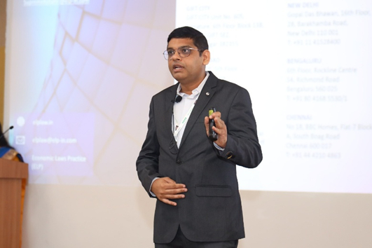
Delivering a presentation on the New BIS Standard for Lab-Grown Diamond Disclosure, Supreme Kothari, Partner, Economic Laws Practice (ELP), informed, “The objective of the new BIS standard is clarity, not conflict. It recognises that natural diamonds and laboratory-grown diamonds are two separate market categories, and therefore requires clear demarcation in terminology so that consumers are not confused about what they are purchasing.”
“The standard also formally recognises that laboratory-grown diamonds have the same chemical composition, crystal structure and physical properties as natural diamonds. At the same time, it prescribes that only ‘laboratory-grown diamond’ or ‘laboratory-created diamond’ can be used for marketing, creating a benchmark for disclosure practices in the industry.”
“While the standard is not mandatory at present, it carries persuasive value. Regulators, consumer courts and marketplaces may rely on it to determine whether there has been misleading advertisement or unfair trade practice under consumer protection laws.”
“On the trade side, laboratory-grown diamonds currently face reciprocal tariffs in the US, and unlike natural diamonds, they are not included in Annex III for automatic exemption. Industry efforts are therefore focused on securing policy parity and clarity under the evolving trade framework.”
The Indian Institute of Gems & Jewellery (IIGJ), an initiative of GJEPC, signed a Letter of Intent (LoI) with InCent-LGD during VAIRAM at IIT Madras to strengthen India’s laboratory-grown diamond (LGD) education and skill ecosystem. The LoI was signed by Debasish Biswas, CEO, IIGJ, and Prof. M.S. Ramachandra Rao, Head, InCent-LGD, IIT Madras. The collaboration will focus on developing joint certification and diploma programmes in LGD technology, integrating industry-oriented training with research-driven academic inputs.
In addition, a book titled Laboratory Grown Diamond – Production Technologies and its Applications, authored by N. Arunachalam, S. Krishnakanth and T. Mukhilan, was also launched on the occasion.
Key Takeaways — InCent-LGD, IIT Madras Introduction by Prof. M.S. Ramachandra Rao
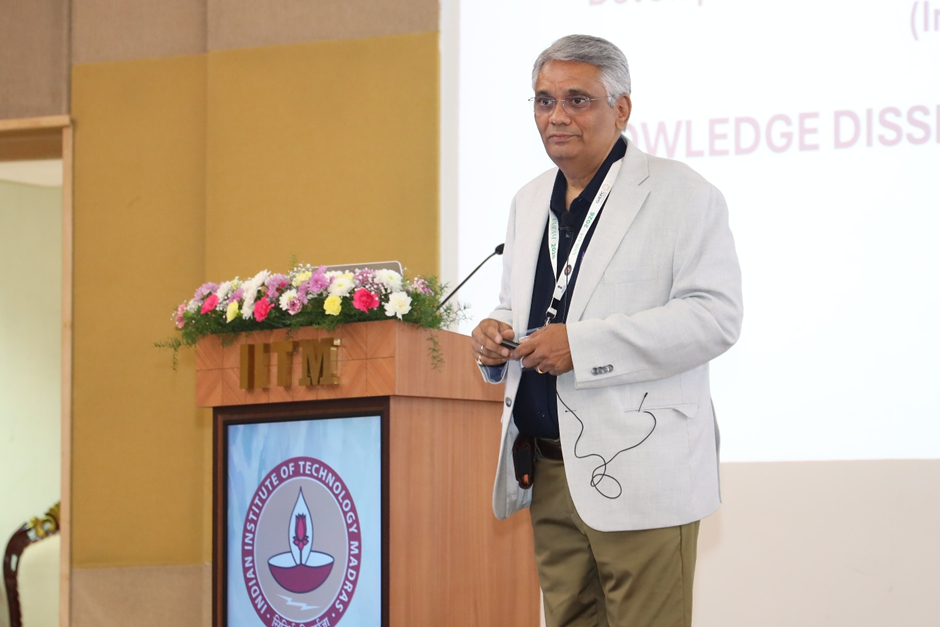
- India is a major LGD producer but lacks core technology ownership
India is the world’s second-largest producer after China, with thousands of MPCVD machines in Surat, yet indigenous HPHT technology and advanced CVD systems remain limited, creating strategic dependence. - InCent-LGD is focused on indigenous machine development
The centre is developing domestic MPCVD (Vajratara) and HPHT (Vajrakaya) systems with complete process recipes to reduce imports and build national capability. - Beyond gems is the long-term strategic direction
Diamond’s exceptional thermal, electrical and optical properties position it for electronics, quantum devices, photonics, power electronics and advanced industrial applications. - High-quality, defect-controlled material is a core research priority
Work is focused on large-area wafers, controlled defects, high-purity growth and characterisation to enable semiconductor and quantum applications. - India needs a full ecosystem, not just growth capacity
Challenges include lack of seed certification, plasma diagnostics, process control and system selection frameworks, which currently limit yield and efficiency across industry. - AI-enabled smart manufacturing is part of the roadmap
Digital twins, machine learning, plasma monitoring and advanced diagnostics are being integrated into next-generation MPCVD systems to improve consistency and productivity. - Diamond marking technology has been developed for traceability
The centre has created VajrĀnkTM, a proprietary laser marking approach below the top surface for seeds and finished diamonds that enables branding and identification (company logos, designs, QR Codes, etc.) without damaging material quality, supporting traceability, authentication and process optimisation. - India has an opportunity to lead in “Diamondtronics”
The presentation highlights the potential for diamond-based electronics, including GaN-on-diamond (gallium nitride), Si-on-diamond (silicon) and quantum NV-centre technologies, with a call to establish a diamond foundry in India. - Commercial translation and industry access are key objectives
The centre aims to provide seeds, process know-how, consulting and technology transfer support to industry partners to accelerate adoption. - Government backing is enabling long-term research investment
The initiative is supported by the Ministry of Commerce & Industry, recognising LGD as a strategic technology sector with high employment and innovation potential.
Key Takeaways — Panel 1: From Diamond Research to Startup Ecosystem
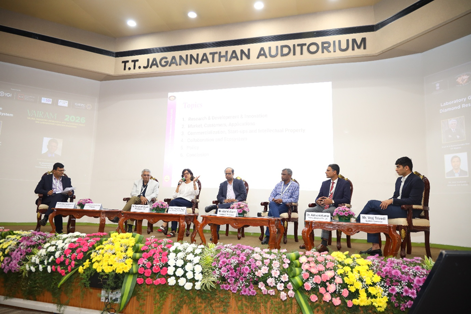
Moderator: Mr. Bharatwaj Ramakrishnan, Former Industry Leader & Semiconductor & Deep-Tech Advisor
Panellists:
- M.S. Ramachandra Rao, IIT Madras
- Tamaswati Ghosh, IITM Incubation Cell
- Bala Prasad Peddigari, Tata Consultancy Services (TCS)
- Atul Kulkarni, Ionbond: IHI Group
- Ashvani Kumar, Pristine Deeptech Pvt. Ltd.
- Vraj Trivedi, Q2-Maitri Diamonds
- India must shift from manufacturing scale to innovation scale
The LGD sector has strong production capability, but future growth depends on translating research into IP, startups and commercial technologies. - IP should be treated as a monetisation tool, not a trophy
Industry is underutilising intellectual property. Protecting IP early and using it as a currency for collaboration can accelerate commercialisation and partnerships. - Collaboration gaps remain the biggest bottleneck
Weak linkages between academia, industry and end-users are slowing technology adoption. Consortium-based models involving institutes like InCent-LGD, BARC and industry were strongly recommended. - Move beyond the “carat economy” toward a technology economy
Diamonds are increasingly valued for functional properties such as thermal management, electronics and quantum applications, requiring a mindset shift across industry. - Commercialisation barriers are more structural than technical
Technology readiness exists, but challenges include capital intensity, investor expectations, government procurement delays and limited pilot-scale infrastructure. - India has a strategic opportunity to lead in next-gen materials
With large CVD capacity and risk-taking entrepreneurs, India can leapfrog into areas like GaN-diamond and advanced electronics if supported by policy push and coordinated investment. - Investing in startups is critical for ecosystem growth
Industry participation as investors and partners in deep-tech startups is essential to convert research into scalable businesses and global products. - Clear strategic direction: “Invent, Validate, Scale from India”
The panel emphasised moving beyond Make in India toward innovation-led global leadership, with calls to convert “carats into qubits” through technology integration.
Key Takeaways — Panel 2: HPHT Diamond Growth: Technology Evolution & Scale-Up
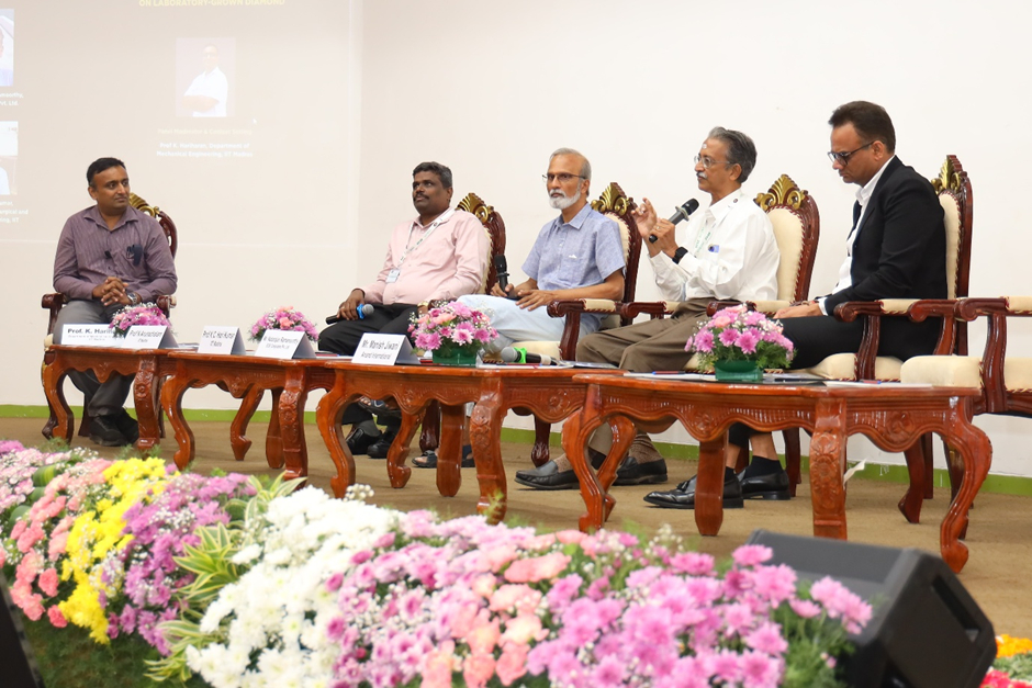
Moderator: Prof. K. Hariharan, Department of Mechanical Engineering, IIT Madras
Panellists:
- N Arunachalam, IIT Madras
- K.C. Hari Kumar, Department of Metallurgical and Materials
- Engineering, IIT Madras
- Natarajan Ramamoorthy, EGS Computers Pvt. Ltd.
- Manish Jiwani, Anand International
- HPHT remains a complex deep-tech challenge
Generating and sustaining ultra-high pressure (5-6 GPa) and temperatures above 1300°C within the reaction volume, while maintaining equipment integrity and process stability, is a major scientific and engineering hurdle. - Supercell design and catalyst behaviour are critical gaps
Limited understanding of catalyst chemistry, material behaviour under extreme conditions, seed preparation and carbon transport mechanisms continues to constrain yield optimisation and scalability. - Indigenous press development is progressing but needs ecosystem support
India is making advances in prototype HPHT systems and supercell components, but scaling to commercial production requires manufacturing ecosystems, supply chains and industry participation. - Reliability, tolerance and process discipline determine commercial viability
Precision engineering, alignment, durability across cycles and cost efficiency are as important as pressure and temperature parameters in achieving sustainable industrial output. - Strong potential for India to replicate CVD success in HPHT
The panel emphasised that India’s entrepreneurial capability, combined with institutional research and policy support, can enable leadership in HPHT technology similar to its rise in CVD production. - Government-industry-academia collaboration is essential
High capex, uncertain ROI and technology risks require coordinated intervention through policy incentives, funding support and joint development programmes to accelerate adoption. - Applications extend far beyond gems
HPHT diamonds have major opportunities across abrasives, sensors, electronics, radiation detection and semiconductor applications, with demand already significant in industrial segments. - Smart manufacturing and AI integration are emerging priorities
Incorporating sensors, data analytics and predictive control into HPHT systems can reduce failure rates, improve yields and optimise energy and material usage. - India faces strategic urgency due to external dependencies
Reliance on imported HPHT machines and potential geopolitical restrictions underline the need for domestic capability development. - Momentum exists, but coordinated execution is the next step
With research institutions advancing rapidly and industry interest growing, the panel concluded that success now depends on sustained collaboration and investment.
Key Takeaways — Panel 3: Lab-Grown Diamonds Beyond Gems – Opportunities, Challenges and Way Forward
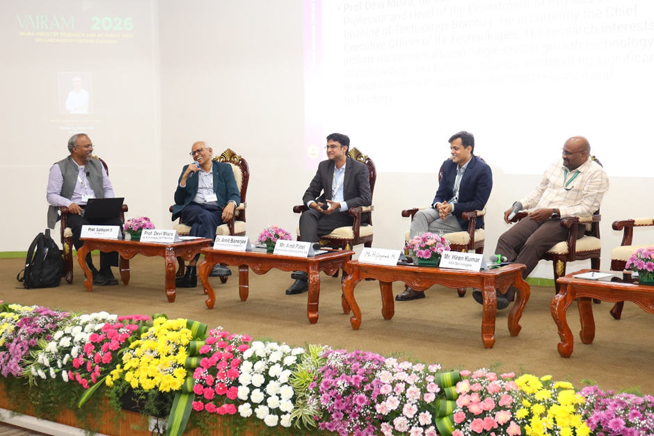
Moderator: Prof. Sathyan S., InCent-LGD, IIT Madras
Panellists:
- Devi Misra, IIa Technologies & IIT Bombay
- Amit Patel, Supreme Green Diamond Pvt. Ltd.
- Amit Banerjee, Microsystem Design-Integration Lab
- Rajaganesh K., InCentLGD, SSMG Group
- Value migration lies beyond substrates toward devices
Moving up the value chain from gem-grade and industrial substrates to functional devices offers significantly higher commercial returns, particularly in electronics, photonics and quantum technologies. - Thermal management and coatings emerge as near-term opportunities
Thermal-grade wafers, heat spreaders, coatings and cutting tools are among the most accessible entry points, leveraging existing CVD infrastructure with moderate process upgrades. - Market creation is as critical as technology development
Even technically viable applications require sustained industry effort to build customer confidence, demonstrate performance and establish commercial demand. - TRL awareness is essential for industry decision-making
Understanding technology readiness levels helps companies assess risk, investment timelines and commercial feasibility when diversifying beyond jewellery applications. - Infrastructure and characterisation gaps are slowing progress
Limited access to advanced testing tools, polishing technologies and post-processing capabilities remains a major constraint for scaling non-gem applications. - Collaboration failures between industry and academia persist
Communication gaps, trust deficits and slow engagement mechanisms are delaying translation from research to commercial products, highlighting the need for structured partnerships. - Corporate labs and consortium models can accelerate innovation
Joint industry-academia facilities, shared infrastructure and coordinated development programmes were identified as effective pathways to bridge the commercialisation gap. - India holds manufacturing scale advantage but must target applications
Existing reactor capacity and process know-how provide a strong base, but success depends on aligning production with specific application requirements rather than generic material output. - Quantum and advanced electronics remain longer-term bets
While sensing applications show promise, large-scale quantum computing and high-end semiconductor integration are still at early development stages globally. - Unified ecosystem action is the central requirement
The panel emphasised joint responsibility across industry, academia and government to convert technical capability into globally competitive products and markets.
Key Takeaways — Panel 4: LGD Quality and Characterisation for Technological Applications
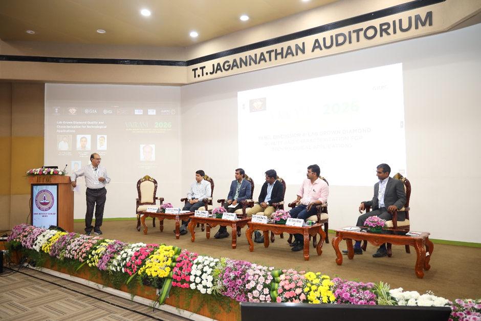
Moderator: Dr. Sairam T N, InCent-LGD, IIT Madras
Panellists:
- Prof Vidya Praveen Ballamudi, IIT Madras
- K.J. Sankaran, CSIR-IMMT, Bhubaneswar
- Tanmay Basu, TCG Crest
- Maneesh Chandran, NIT Calicut
- Nikhil Alfred, IGI
- Technology applications require new grading frameworks
Existing gemological standards are inadequate for deep-tech use cases, creating an urgent need to define electronic-grade, thermal-grade and quantum-grade classification based on material performance and defect levels. - Characterisation is as critical as growth technology
Reliable measurement of defects, impurities, surface functionalisation and crystallographic quality is essential to validate materials for high-tech deployment and commercial adoption. - Diamond properties often exceed equipment limits
Extreme hardness, thermal conductivity and insulating behaviour make characterisation technically difficult, with many standard instruments unable to measure high-quality material accurately. - Advanced infrastructure gaps are slowing progress
Access to high-end tools such as SIMS, high-resolution spectroscopy and specialised thermal measurement systems remains limited, constraining research and industrial translation. - Shared consortium facilities offer the most practical solution
Centralised characterisation hubs supported by industry-academia collaboration are more viable than individual companies investing in expensive equipment with limited utilisation. - Defect engineering enables next-generation applications
Controlled impurities and engineered defects are fundamental for quantum sensing, photonics, electronics and electrochemical technologies, shifting defects from a limitation to a functional asset. - Industrial trust depends on validated benchmarking data
Credible specification sheets, third-party testing and standardised benchmarking are necessary to build confidence between academia and industry and accelerate technology transfer. - Multiple form factors expand application potential
Polycrystalline coatings, nanostructured diamonds, doped electrodes, thin films and bulk single crystals each serve different industrial and technological applications. - Surface engineering and adhesion remain major challenges
Coating adhesion, substrate compatibility, polishing and impurity control continue to limit scalability for mechanical and electronic applications. - Certification and detection technologies are evolving with AI
Machine learning-based detection and fluorescence analysis are improving LGD identification, though rapid process changes by growers create ongoing challenges.